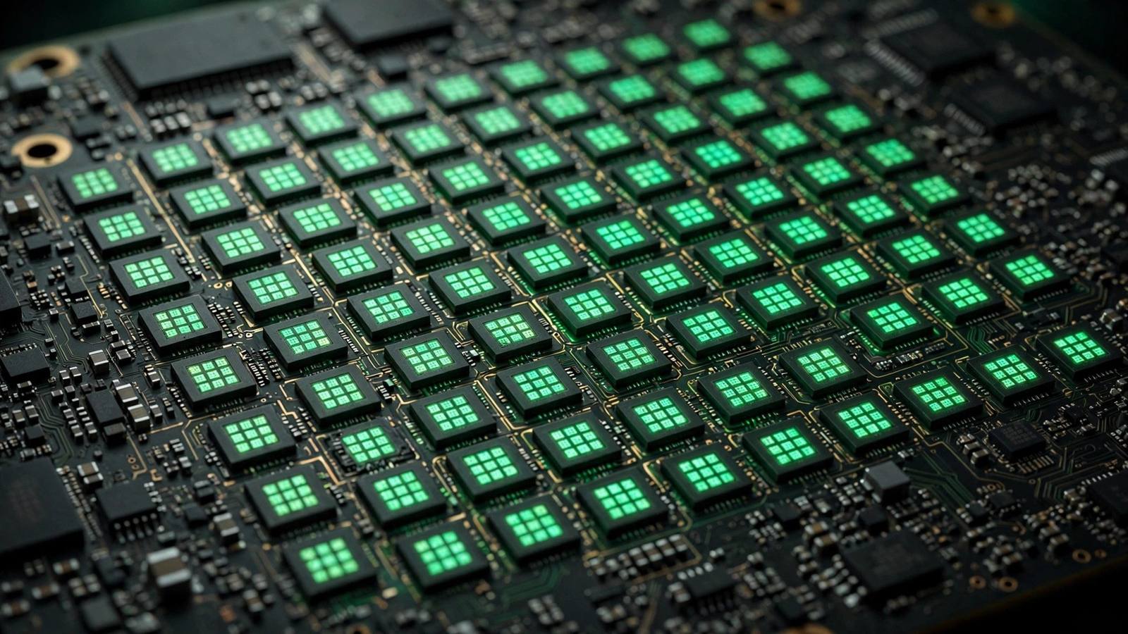
On October 12, 2026, SK hynix's H-TPU had its architecture detailed at the International SoC Design Conference (ISOCC 2026) in Incheon, South Korea. It is an ultra-lightweight programmable processor the company developed in-house for solid-state drive controllers. A single H-TPU consumes roughly 2.5 percent — one fortieth — of the power of a general-purpose CPU core and occupies about 4 percent — one twenty-fifth — of the chip area, and a single controller integrates more than one hundred of them.
Why big CPUs no longer fit SSD controllers
Most of the work inside an SSD controller is simple and repetitive: read and write command processing, metadata management and buffer control. General-purpose CPU cores have traditionally handled all of it, but as drives got faster, more cores were needed, and chip area and power consumption ballooned with them. SK hynix vice president Koo In-je said at the conference that the Arm cores commonly used in SSD controllers are overpowered for such tasks: they are designed for complex, high-speed computation, so using them for small repetitive work wastes power and area, and their architecture is poorly suited to splitting jobs across many processors. The H-TPU therefore uses a four-stage pipeline and a sequential execution structure tuned for repetitive I/O paths. The general-purpose CPU is not removed from the controller; it steps back and handles only genuinely complex work such as error recovery, exception handling and storage policy management.
Waking on demand instead of burning power together
More than one hundred H-TPUs are distributed across the controller, each assigned to specialized functions. When an I/O request arrives, only the units responsible for the needed functions are activated, while the rest stay idle to save power. SK hynix has also built software tools for the architecture, including a dedicated compiler, so engineers can write specialized code for these small processors more efficiently. In essence, the design copies at the storage layer what data centers have been doing for years: instead of chasing one all-powerful core, let many specialized units each handle a small slice of work.
Rollout order: enterprise SSDs first, then AI storage
According to the plan presented at the conference, H-TPU will first appear in controllers for next-generation enterprise SSDs, then move into Storage Next, the company's next-generation storage architecture for AI, and into high-bandwidth flash (HBF), which is scheduled for release next year. Storage Next is designed for the fine-grained data access modern AI models require, handling data units as small as 512 bytes — one eighth of the conventional 4KB unit. Inference services increasingly depend on how storage responds, with model weights, KV caches and retrieval data flowing constantly between drives and memory, so controller-level power and scheduling efficiency show up amplified on the whole-system bill. SK hynix gave no mass-production timeline, and the figures disclosed are the company's own; the real gains will have to wait for measurements once the first enterprise SSDs ship. The direction itself is still notable: the AI infrastructure power-saving race has now reached the SSD controller.